Soldering and PCB Design: How Thermal Dynamics Influence Circuit Reliability
In the ever-evolving field of electronics manufacturing, the intersection between PCB design and soldering techniques plays a critical role in determining overall circuit reliability. Whilst PCB design governs the structural and electrical integrity of a board, the soldering process ensures the secure and conductive placement of components. This synergy is especially sensitive to thermal dynamics. Inadequate thermal management can compromise solder joints, accelerate component fatigue, and ultimately cause premature system failure. As devices shrink and power densities increase, understanding how design decisions affect thermal behaviour and soldering outcomes is not only valuable, it is essential.
Understanding Thermal Dynamics in PCB Design
Effective thermal management is a foundational aspect of modern PCB design and is a key topic covered by IPC training providers. As components become more compact and power consumption rises, heat generation within a printed circuit board increases significantly. This thermal load, if unmanaged, can degrade solder joints, shift component values, and cause delamination or warping of substrates. To mitigate these risks, PCB designers use techniques such as thermal vias, copper pours, and multi-layered ground planes to disperse heat away from sensitive areas. The thermal conductivity of the base material, typically FR-4 or polyimide, also plays a decisive role in overall heat dissipation capacity.
Strategic component placement and trace routing further influence how heat is distributed. High-power devices such as voltage regulators and microprocessors should be positioned with adequate spacing and aligned with efficient airflow paths. Incorporating heat sinks, thermal pads, and managing power-to-area ratios are also essential tactics. These design considerations are not isolated from soldering processes; rather, they shape how soldering techniques perform under real-world thermal stress. Without precise thermal analysis during the layout phase, even well-soldered joints may fail under sustained operating conditions.
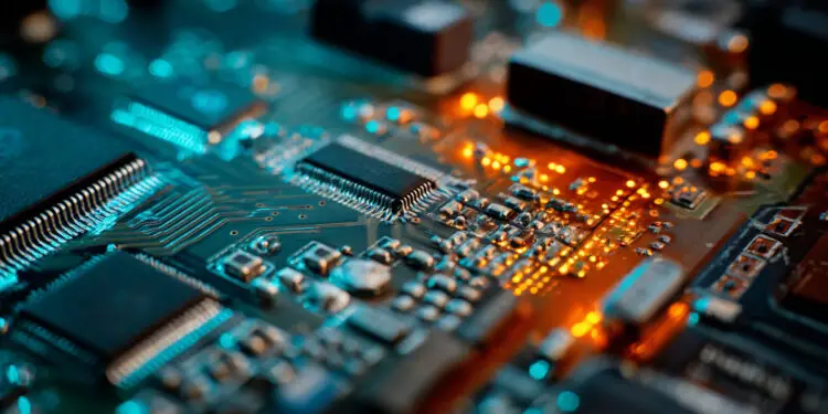
Soldering Techniques and Their Thermal Implications
The choice of soldering technique directly influences how a PCB responds to thermal stress, both during assembly and in operational use. Reflow soldering, the most prevalent method in surface mount technology, relies on a controlled temperature profile to gradually heat components and solder paste before cooling in a highly regulated manner. In contrast, wave soldering immerses the underside of the board into a molten solder wave, primarily used for through-hole components. Hand soldering, often reserved for rework or low-volume applications, introduces higher variability in temperature and dwell time. Each technique imposes distinct thermal loads that must be accounted for in the PCB layout to prevent thermal shock or uneven heat distribution. Understanding these interactions is a critical part of professional development, and working with an experienced electronics training provider can significantly enhance a technician’s ability to apply the correct process for the design at hand.
Design features such as pad size, copper density, and thermal relief patterns significantly affect soldering outcomes. Larger copper pours can act as heat sinks, drawing thermal energy away from joints and causing incomplete solder wetting or cold joints if not properly compensated for in the soldering profile. Thermal relief pads, which isolate pads from surrounding copper with narrow connections, are often introduced to reduce heat sinking during soldering and ensure consistent joint formation. A synergy between design and process control is essential to achieve repeatable, high-quality solder joints that withstand operational stresses.

Designing for Thermal Reliability
Ensuring thermal reliability in PCB design requires a proactive approach that considers not just the immediate requirements of soldering but also the long-term performance of the circuit under variable thermal loads. Designers must account for current-carrying capacity through accurate trace width calculations, which are influenced by copper thickness and allowable temperature rise. IPC-2221 standards offer established guidelines for these parameters, though many engineers supplement them with simulation tools to predict hot spots and thermal gradients across complex multilayer designs. Material selection is equally important; high-Tg substrates provide improved stability under elevated temperatures, while metal-core PCBs are increasingly employed in power-intensive applications for their superior thermal conductivity.
Another critical aspect is the use of thermal relief structures and component spacing to mitigate heat accumulation. Closely packed components without adequate ventilation or copper balancing can experience differential heating, leading to mechanical stress and solder fatigue. Thermal vias, when properly connected to internal copper planes, help draw heat away from high-power devices and reduce localised temperature build-up. These techniques are not merely best practice; they are essential for maintaining the integrity of solder joints and ensuring product reliability in real-world environments where thermal cycling and power surges are routine.
Conclusion
The interplay between PCB design and soldering is inseparable from the question of thermal reliability. Decisions made at the layout stage have lasting consequences on how a circuit performs under thermal stress, impacting everything from joint integrity to component lifespan. By integrating design techniques such as thermal vias, relief pads, and precise material selection with well-matched soldering processes, engineers can significantly enhance circuit resilience. For professionals working at the interface of design and manufacturing, developing a strong understanding of these principles is not only beneficial, it is indispensable to producing robust, high-performance electronics.